EAGLE Tutorial - Part 2 - Schematic editor
Introduction
In this tutorial, the reader will be guided to create a simple PCB. This page is the part 2 of the tutorial, dedicated to the schematics editor.
Workspace
Before starting the schematic, lets insert a frame containing title, date, author... On the vertical tool bar located on the left side of the window, click on the ADD icon. The ADD action allows to add new item in the design. It is largely dedicated to the insertion of new components.
![]()
A window pops up and display all the available libraries. In the search entry located at the bottom left of the window, type “frame” and confirm with the Enter key :

The list of libraries is now limited to entries containing the string “frame” in there title or description. Select the A4L-LOC which is a DIN A4 Landscape frame and click OK. The frame is now attached to the cursor, place the frame in order to align the bottom-left corner of the frame at coordinates 0,0. Coordinates are displayed in the upper left corner of the working area. The origin is also display in the working area with a small dotted cross. When the frame is placed, left click with the mouse and hit twice the “Esc” key to exit.

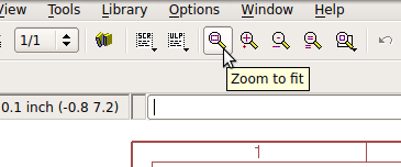
Save your design and change the view by clicking on “Zoom to fit”. You should now have a general view of your future design.
Click on the grid icon:

The grid setting window appears, in this window, you can set the grid parameters (size, style, etc.). Set display “On” and click “OK”. Your workspace is prepared for the schematic and should look like this:

Adding symbols
Click to the ADD icon as explained previously for adding the frame. EAGLE is provided with a large number of librairies, and the user can enter one or more search patterns in the search field by using special characters (wild cards) ? and *:
- * is a search pattern that can be replaced by one or several characters. For example *555 will provide all the entries ending by 555. 555* will provide all the entries beginning by 555 and *555* will provide all the entries containing 555.
- ? is a search pattern similar to *, excepted that it can only be replaced by a single character.
It is usefull to remember that when you add a device, right click rotate and left click place the symbol. Once a symbol is placed, several operations are still possible :
| Move | Copy | Rotate | Delete |
|---|---|---|---|
 |
 |
 |
 |
Search and add the following components in your design:
| Component | Library | Device | Package |
|---|---|---|---|
| 555 timer | st-microelectronics | NE555 | DIL-08 |
| Resistor | rcl | R-EU | 0204/7 |
| Polarized capacitor | rcl | CPOL-EU2,5-6E | E2,5-6E |
| Capacitor | rcl | C-EUC1206 | C1206 |
| Screew terminal | con-ptr500 | AK500/2 | AK500/2 |
| 5mm LED | led | LED5MM | LED5MM |
| VCC supply symbol | supply2 | VCC | - |
| GND supply symbol | supply2 | GND | - |
Note that, even if VCC and GND are provided for convience and are not real components, they can be found in the libraries. Add and place your components in order to get the following arrangement:

Adding connections
The electrical connections have to be drawn with the NET tool (or the bus tool for buses). The WIRE tool also draw lines, but it is not dedicated to electrical connections, it belongs to the drawing tools (text, circle, arcs…).
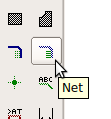
Once the NET tool is selected, add a connection by clicking on the first pin to connect. Place the cursor on the second pin or junction, and right click without moving the mouse: the wire bend style will automaticaly change. It can also be done by selecting one of the wire bend style icon:

Place the connection according to the following schematic. This is a very simple NE555-based LED blinker:

Component name and value
The following icon (NAME) allows the user to change a component name:

In the same way, the VALUE icon allows the user to add or modify the component value (when applicable):

Rename and set values of each symbol according to the following illustration:

Check errors
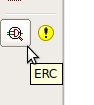
Once your schematic is finished, it is safe to use the ERC (Electric Rules Check) tool. It can detect many mistakes in the design (wrong connections, non compatible junctions …)
A new window pops up, and displays four warnings:

The first one says that the pin 8 of the NE555 is called VCC+ and is connected to VCC. The three others say that the frame, the LED and the screw terminal don’t have values. As none of this four warning is an error, the four errors can be approved. The dialog box should now display zero error, zero warning and four approved:

Generating board
When the schematic is finished and checked, the board can be created. Click on the following icon to generate the board and launch the board editor.

EAGLE may ask you to confirm the creation of a new board from your schematic, answer yes and the PCB is automatically prepared for routing:

See also
- Adding copper pour in EAGLE
- Adding mounting holes to a PCB with EAGLE PCB software
- Create Solidworks 3D model from EAGLE
- EAGLE Tutorial - Part 1 - Control panel
- EAGLE Tutorial - Part 3 - Board editor
- EAGLE Tutorial
- Install EAGLE 6.6 on Ubuntu 16.04
- Understanding layers in EAGLE PCB Software
- Usefull EAGLE ULP scripts