Understanding layers in EAGLE PCB Software
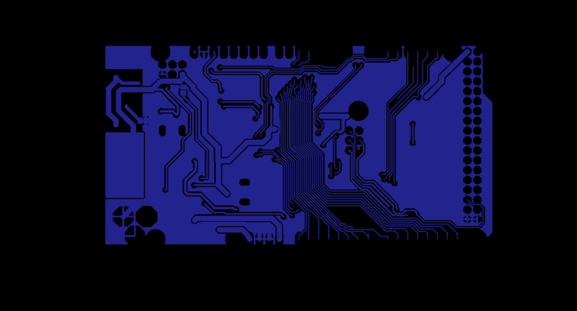
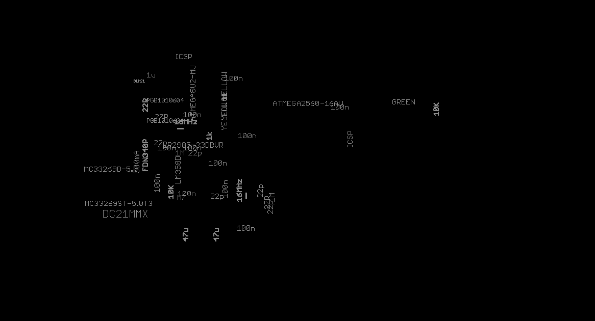
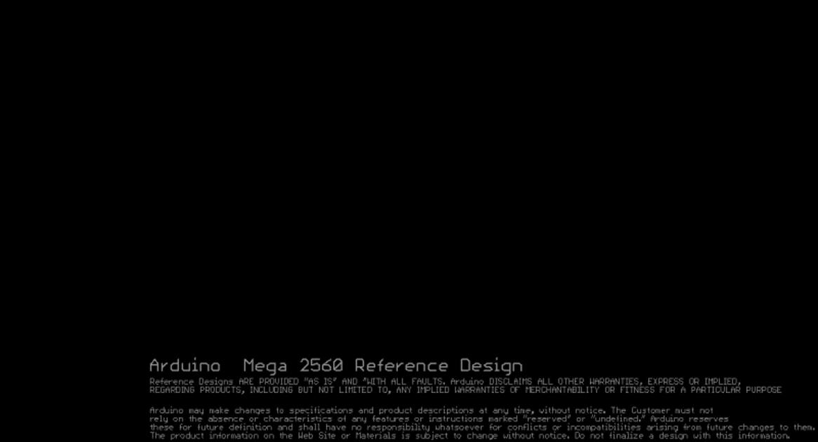
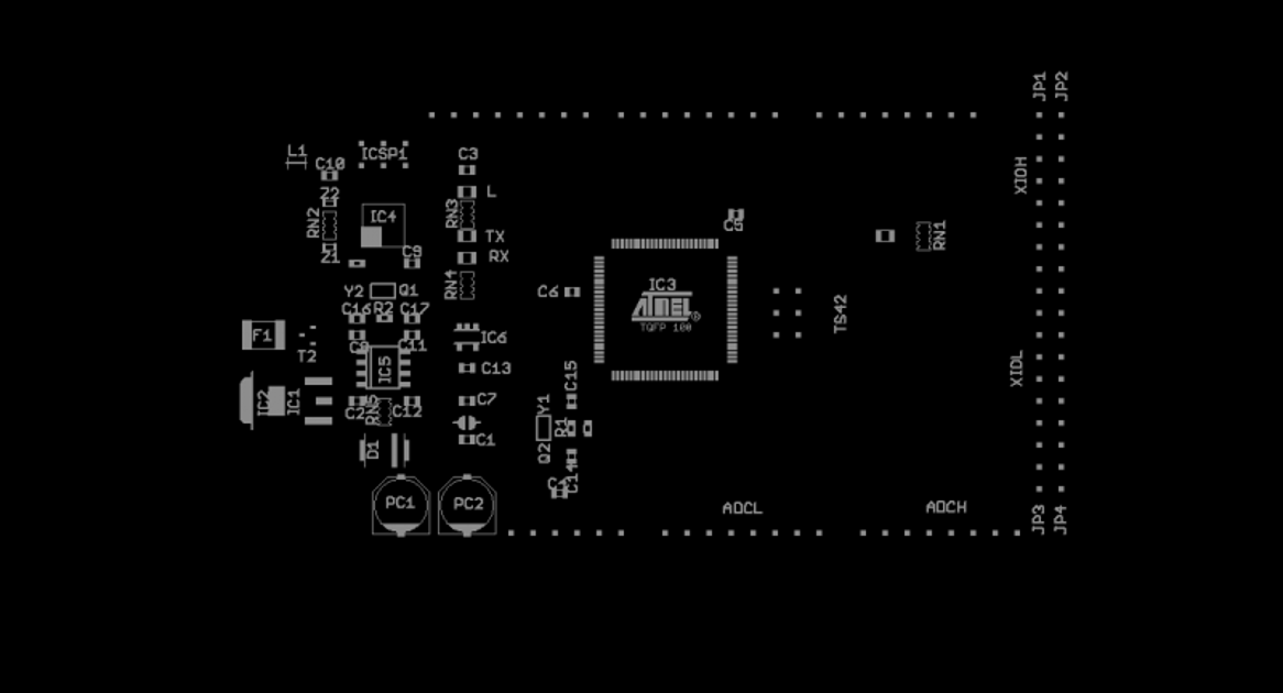
Each layer in EAGLE is dedicated to a given function. Placing each item in the appropritaed layer is highly recommanded. This article presents each layer and describes it functionality. The famous Arduino MEGA 2560 board is taken as example. Note that the picture is not exactly identical to the PCB, but is quite enough to understand each layer:
| Arduino Mega | CAD view of the Arduino Mega |
|---|---|
 |
 |
Layer 1 - Top
The first layer contains the top side tracks and the top side copper pour (if used).

Layer 2 to 15 - Route
This is the inner layer tracks (only for multilayer PCB).
Layer 16 - Bottom
This layer contains the bottom side tracks and the bottom side copper pour (if used).
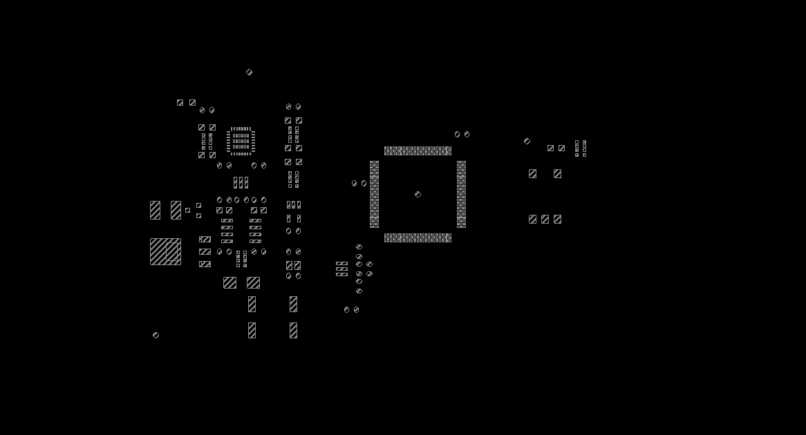
Layer 17 - Pads
This layer contains the through-hole pads.

Layer 18 - Vias
This layer contains the through-hole vias.

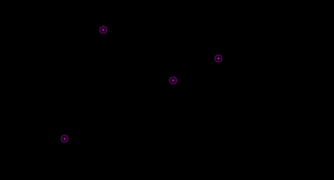
Layer 19 - Unrouted
This layer contains the unrouted tracks, i.e. the airwires (rubberbands). Here almost all the board is routed, there is just a few unrouted tracks:

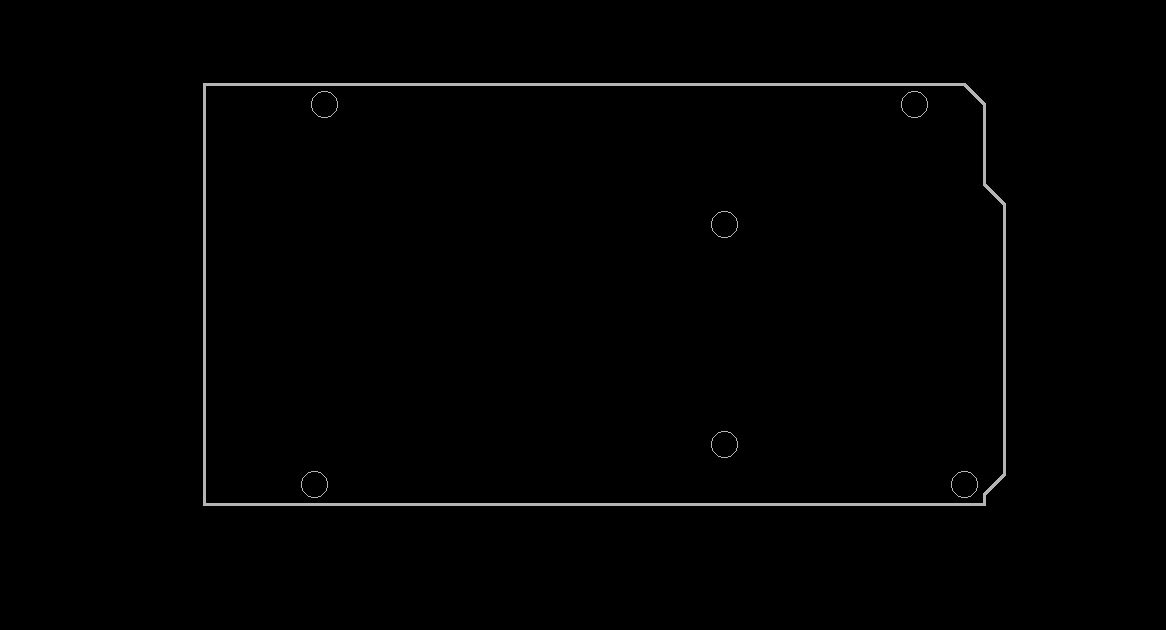
Layer 20 - Dimension
This layer contains the board outlines and circle for holes.
Layer 21 - tPlace
This layer contains the top side silk screen. It usualy contains the component outlines. Care must be taken not to cover any ares that have to be soldered. It is also possible to create additional and rather betterlooking silk screen for documentation purposes in layer 51, tDocu. This may indeed cover soldered areas, since it is not output along with the manufacturing data.
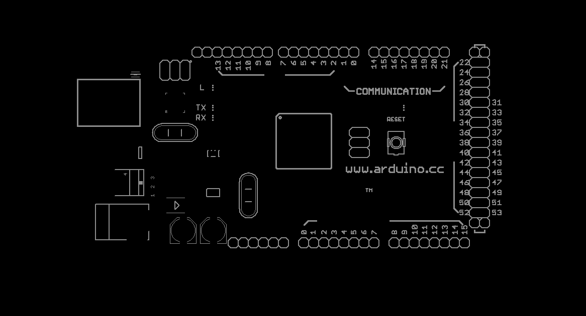
Layer 22 - bPlace
This layer contains the bottom side silk screen (see layer 21 for more details).
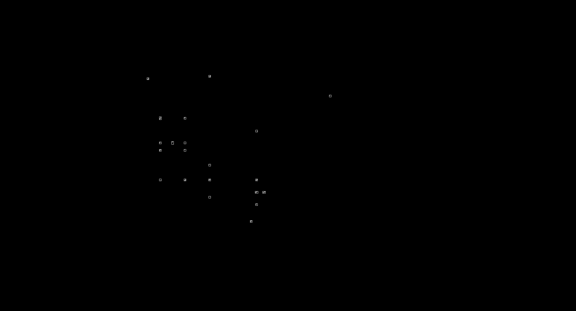
Layer 23 - tOrigins
This layer contains the top side component origins. It contains the origin cross for each component. Top side components can be moved or modifyed only if this layer is visible.

Layer 24 - bOrigins
This layer contains the bottom side component origins (see layer 22 for more details). Bottom side components can be moves only if this layer is visible.
Layer 25 - tNames
This layer contains the top side service print. It usualy contains the component names and may appear on the PCB as the silk screen.
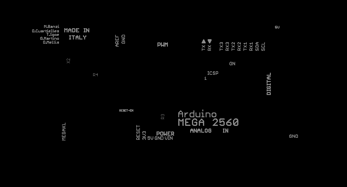
Layer 26 - bNames
This layer contains the bottom side service print (see layer 25 for more details).
Layer 27 - tValues
This layer contains the top side component value. It usualy contains the component value and appears on the PCB as the silk screen and service print.
Layer 28 - bValues
This layer contains the bottom side component value (see layer 27 for more details).
Layer 29 - tStop
This layer contains the top side solder stop mask (solder mask). This is the nogo area for the green laque. Data is implicitly created for THT and SMD pads, and optionally VIAs (depending on settings).

Layer 30 - bStop
This layer contains the bottom side solder stop mask (see layer 29 for more details).
Layer 31 - tCream
This layer contains the top side solder paste data for SMD, normally used to make stencils for printing the paste to the board before assembly. Data is implicitly created with SMD pads. This area should be a little smaller that the solder stop mask because the green laque shouldn't overlap solder areas.
Layer 32 - bCream
This layer contains the bottom side solder cream (see layer 31 for more details).
Layer 33 - tFinish
This layer is dedicate to special finishing process (plated gold, silver carbon. It may also be used if some of the pads need immersion gold plating. It is not automaticaly generated and it must be drawn by designer.
Layer 34 - bFinish
This layer contains the bottom side finish data (see layer 33 for more details).
Layer 35 - tGlue
This layer contains the top side glue mask. For wave soldering of SMD parts, they must be glued to the board first. Usually, one small dot in the center of chips, and several dots under IC packages are used. This layer must be drawn by the designer, normally when designing the libraries.
Layer 36 - bGlue
This layer contains the bottom side glue mask (see layer 35 for more details).
Layer 37 - tTest
This layer is the top side test and adjustment. It is dedicated to testpoint for ICT (In Circuit Test).
Layer 38 - bTest
This layer is the bottom side test and adjustment. It is dedicated to testpoint for ICT (In Circuit Test).
Layer 39 - tKeepout
This layer is the top side keepout area for components. Components should not be placed in this area (except for part ower of the area).
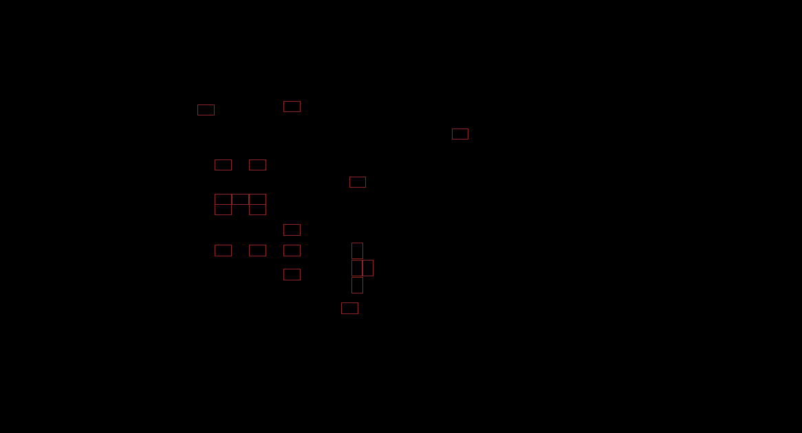
Layer 40 - bKeepout
This layer is the bottom side keepout area for components (see layer 39 for more details).
Layer 41 - tRestrict
This layer is the top side keepout area for tracks. Tracks should not be placed in this area.
Layer 42 - bRestrict
This layer is the bottom side keepout area for tracks (see layer 41 for more details).
Layer 43 - vRestrict
This layer is the keepout area for vias.
Layer 44 - Drills
This layer contains the conducting through holes. It is usually used for pads (of through hole components) and vias.

Layer 45 - Holes
This layer contains the non-conducting holes. It is usually used for s used for mounting holes.

Layer 46 - Milling
This layer is dedicated to milling. If the board manufacturer has to mill oblong holes, you have to draw the milling contour of oblong holes in this layer. Any other inner cutouts in the board are drawn in the same way. Draw the milling contours in this layer. Note that the board outline is not concerned and must be designed in the layer 20 (Dimension).
Layer 47 - Measures
This layer contains the measurement. It is not used during the manufacturing process, it is just display for information.

Layer 48 - Document
This layer contains the general documentation. Had here comments, or any usefull information that help understanding the design of the PDB.
Layer 49 - Reference
This layer contains the reference marks and is typicaly used for placing the fiducial marks. Fiducials are little target registration marks that are printed on PCBs, they are placed on the top copper layer (and bottom if you're doing 2-layers) and allow the vision system of the pick and place to recognize where the PCB is at. They are not placed on the mask or silk because they are not as precisely aligned to the parts as the copper itself.
Here is a picture from Lady Ada (Adafruit company) that illustrate the automatic localization process of the fiducial marks (photo courtesy of Lady Ada / Adafruit company):

Layer 51 - tDocu
This layer contains the top side part documentation. Place additional graphical information for the documentation here. This layer is not used to print onto the board itself, but is a supplement to the graphical presentation which might be used for printed documentation. Care must be taken in layer 21, tPlace, not to cover any areas that are to be soldered. A more realistic appearance can be given, however, in the tDocu layer, which is not subject to this limitation.
Layer 52 - bDocu
This layer contains the bottom side part documentation (see layer 51 for more details).
See also
- Adding copper pour in EAGLE
- Adding mounting holes to a PCB with EAGLE PCB software
- Create Solidworks 3D model from EAGLE
- EAGLE Tutorial - Part 1 - Control panel
- EAGLE Tutorial - Part 2 - Schematic editor
- EAGLE Tutorial - Part 3 - Board editor
- EAGLE Tutorial
- Install EAGLE 6.6 on Ubuntu 16.04
- Usefull EAGLE ULP scripts